Semiconductor Equipments
|
Mask Aligner
Spin coating Systems
Chemical Mechanical Planarization (CMP):
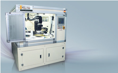
G&P Polishing system is designed to polish a wafer to planarization patterned surface as well as to smooth surface roughness of semiconductor materials. The systems can accommodate three to twelve inch diameter wafers. Polishing process parameters can be adjusted including Polishing pressure, Retainer pressure( only for membrane type head), Rotational speed of the polishing platen, Rotational speed of the rotational head, rotational speed of the conditioning head , Oscillation on / off. Plasma Enhanced Chemical Vapor Deposition (PECVD):
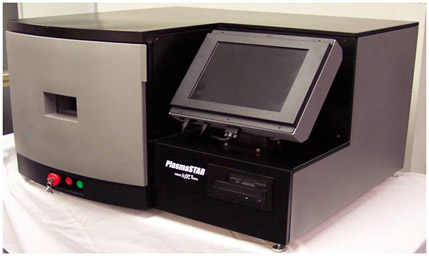
It is a unique plasma processing system capable of Parallel Plate PECVD plasma processing. The system will accommodate up to eight (8) inch substrates or a variety of smaller substrate sizes and shapes. The system is designed to provide a wide range of plasma operating conditions and is ideally suited for research, process development or low volume production. The small system footprint allows for easy installation in a laminar flow hood or on a work bench. The system is designed with many standard features not found on other systems in it's size or price range.
Reactive Ion Etching System & Deep Reactive Ion Etching System: 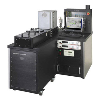
- ICP Source for High Rate Process
- DRIE – Compound semiconductor materials, metals, Si, SiO2, Si3N4
- Low / No Damage Etch – Vertical Walls
- PECVD – Low Stress, Low Temperature SiO2, Si3N4, SiOxNy
- 1 KW, 13.56 MHz RF ICP Power (optional 3 KW)
- 600W, 13.56MHz RF Bias Power
- Automatic Matching Network
- Downstream Pressure Control
- Turbo and mechanical pumps
- PC Control with Windows Operating System
- Recipe Driven Programming with Graphical Presentation
Plasma Asher:
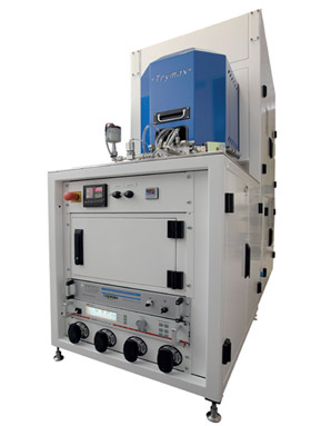 Trymax NEO series can accommodate upto 300mm diameter wafer is an advanced tool for etching and ashing process. Semi auto and fully automated single chamber systems. It produces excellent uniformity and repeatability, throughput > 100 wph.
Application includes: Bulk Resist Strip, Descum processing , Polymer removal, Post High dose Implant strip, Silicon Nitride Etch applications, MEMS applications, Backend Packaging process. Trymax NEO series can accommodate upto 300mm diameter wafer is an advanced tool for etching and ashing process. Semi auto and fully automated single chamber systems. It produces excellent uniformity and repeatability, throughput > 100 wph.
Application includes: Bulk Resist Strip, Descum processing , Polymer removal, Post High dose Implant strip, Silicon Nitride Etch applications, MEMS applications, Backend Packaging process.
Sputtering Systems:
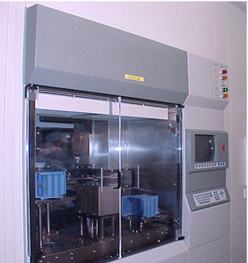
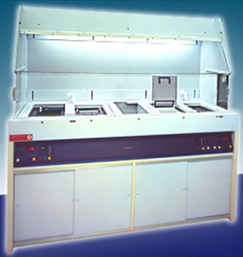
Wet Benches:
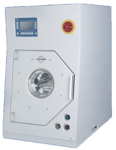
Spin Dryer:
|
|
|